


Bitcoin trading bot httpsyadiskdnbghmsru3uluzd
37 comments
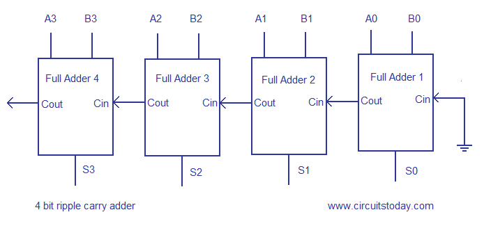
16 bit ripple carry adder verilog code
This is an open access article distributed under the Creative Commons Attribution License , which permits unrestricted use, distribution, and reproduction in any medium, provided the original work is properly cited. The design of a bit carry-skip adder to achieve minimum delay is presented in this paper. A fast carry look-ahead logic using group generate and group propagate functions is used to speed up the performance of multiple stages of ripple carry adders.
The group generate and group propagate functions are generated in parallel with the carry generation for each block. The optimum block sizes are decided by considering the critical path into account. The new architecture delivers the sum and carry outputs in lesser unit delays than existing carry-skip adders. The adder is implemented in 0. The critical delay for the proposed adder is 3.
The simulation results show that the proposed adder is 18 faster than the current fastest carry-skip adder. The ever-increasing demand for mobile electronic devices requires the use of power-efficient VLSI circuits. Computations in these devices need to be performed using low-power, area-efficient circuits operating at greater speed. Addition is the most basic arithmetic operation; and adder is the most fundamental arithmetic component of the processor.
Depending on the area, delay and power consumption requirements, several adder implementations, such as ripple carry, carry-skip, carry look-ahead, and carry select, are available in the literature [ 1 , 2 ]. The ripple-carry adder RCA is the simplest adder, but it has the longest delay because every sum output needs to wait for the carry-in from the previous full-adder cell.
It uses area and a delay of for an n-bit adder. The carry look-ahead adder has delay and uses area. On the other hand, the carry-skip adder and carry-select adders have O v n delay and use area [ 3 ]. In this paper, we present the design of a low-power adder with less delay while using minimum hardware. The standard carry generate-propagate logic is used to reduce the critical delay of the adder while blocks of RCAs are used for lesser power consumption.
In our design, the generate-propagate logic balances the delay and the number of inputs to the skip logic limits the critical path delay. In Section 2 , we will discuss the previous work done in the area of high-performance adders. In Section 3 , we present the design of our adder. Section 4 presents the design of a few basic CMOS cells used in the adder. In Section 5 , we present the simulation results for our adder and compare it to other fast adders.
The design of a carry-skip adder is based on the classical definition of generate and propagate signals as follows [ 1 , 2 ]: The carry out from the th adder cell is expressed as where is the carry input to the th cell. Two signals, group generate and group propagate, are also defined in [ 1 , 2 ] and are given by where and are group generate and group propagate signals from th cell to th cell, respectively.
Then, the expression for carry out from the whole group is given by. Different adder implementations have been developed to optimize various design parameters. Most adder implementations tend to trade off performance and area.
It is a variation of the basic carry look-ahead adder. They emphasized the need for regularity in VLSI circuits to reduce design and implementation costs. They use two types of processor cells: The black processor performs the associative concatenation defined in [ 5 ] and the white processor simply transmits the data. The adder delay was calculated in terms of the number of exclusive-or XOR operations performed while treating each XOR delay as one unit time.
For an n-bit adder, the Brent-Kung adder has a delay of and uses area. The black and white cells are quite similar to the ones used in Brent-Kung adder. They divided the n-bit adder into ascending and descending halves so as to limit the number of bits in the final stage. The concentration of the maximum number of bits was in the middle of the adder and was defined as the height of the adder. The algorithm ends up in an unbalanced binary tree with a delay of consuming an area.
The ELM-adder design presented in [ 7 ] computes the sum bits in parallel; thereby reducing the number of interconnects. It implements an n-bit adder as a tree of processors to directly compute the sums in time. The area used is. The adder design was expressed in terms of standard cells, which do not compute carry for each stage. Instead, partial sums were computed for each stage. The fan-in to the carry-skip logic increases linearly towards the middle of the adder.
A two-level carry-skip adder is presented in [ 9 ], where the whole adder stage is divided into a number of sections, each consisting of a number of RCA blocks of linearly increasing length. These adders reduce the delay at the cost of an increase in area and less regular layout. RCA was concluded to have utilized the least power, but has the highest delay due to its carry chain. A variable-width carry-skip adder was shown to be superior to constant-width carry-skip adder, the advantage being greater at higher precisions.
To reduce delay and power consumption, the adder is divided into variable-sized blocks that balance the inputs to the carry chain. The main principle behind this design was to utilize the lower blocks and make them work in parallel with higher blocks. This paper is a deviation from the tree approach presented in the ELM adder.
A bit adder implementation with a delay of 7 logic levels using carry-skip adders and ripple-carry adders was presented in [ 4 ]. This is shown in Figure 1. The logic-level delay defined in the paper is equivalent to the delay of a complex CMOS gate. The bit adder is divided into 4 adder blocks as shown in Figure 1. Carry-select adders were used in the final CS4 block, which significantly increases the hardware.
The paper claims that the output will be ready with a delay of 7 logic levels, with the assumption that the critical delay path is the carry propagation path of bit. But a closer examination of the previous block CS18 reveals that the th bit of the sum output will be available only after a delay of 9 logic levels. The complete adder is divided into a number of variable-width blocks. The width of each block is limited by the target delay T.
Each block is further divided into subblocks. A subblock may contain additional levels of subblocks in a recursive manner. The lowest-level subblock is formed by a number of variable width RCAs. The adder structure is described as follows:. The bit adder is divided into four blocks. A block diagram of the first three blocks is shown in Figure 2. The first block LSB is a full adder by itself.
The carry from the first block is fed into the second block and is also fed into the skip logic. The generate and propagate functions are generated separately for each full adder in one unit time, where one unit time is defined as the delay of a complex CMOS gate with at most three transistors connected in series from the output node to any supply rail.
In Figure 2 , the numbers shown in parenthesis represent the number of unit delays of the signal arrival times at the appropriate signal leads. Since the delay of a complex CMOS gate is quadratic on its stack height, in our design, the stack height is limited to 3. This also restricts the maximum number of inputs to the carry-skip logic to 7. On the other hand, when the generate-propagate outputs are used for group generation and group propagation outputs, a stack height of 3 in the CMOS implementation will allow a 4-bit RCA.
The carry-generation delay from the skip logic is minimized by alternately complementing the carry outputs. Hence, the carry signals generated are and so forth. For the very first 1-bit block , the carry-generation logic is more important than the sum-generation logic since the overall delay of the adder is dependent on the carry from this block.
Hence, this block is designed by minimizing the carry out delay as much as possible. The simplest expression of carry out from the LSB full adder is given by where and are the operand bits and is the input carry. An AOI gate implements this. The block in Figure 2 is implemented as a k-bit RCA.
For any k-bit RCA, the total number of propagate and generate outputs would be 2? The fan-in restriction of 7 to the carry-skip logic therefore limits the number of bits in the RCA to 3.
The final Sum output from this 3-bit RCA will be available in 4 time units. The sum outputs for this RCA are generated either as or depending on the carry signal value The carry out and are implemented as and respectively. Now consider block in Figure 2. The delay of carry signal arriving at the input of the skip logic is 2 time units. This implies that the group generate-propagate logic outputs feeding the skip logic must also be available in 2 time units.
Hence, the inputs to the logic must be available in 1 time unit. This implies that the inputs to the logic must be the propagate and generate signals of the full adders. Block is divided into three subblocks and in this case, each subblock is an RCA. The maximum width of each RCA is limited to 4 bits due to the fan-in restrictions imposed on the block. The width of each RCA is also limited by the target delay of the bit adder. The width of the first RCA is given as where is the arrival delay of the carry output from the previous block.
The width of all remaining higher order RCAs in the same block will be 1 bit less because of the delayed arrival times of their carry input by an additional time unit. For a target delay of 6 time units, the width of the first RCA in is 4 bits and the widths of the remaining RCAs are each 3 bits. The number of RCAs in is limited to 3 due to the fan-in restriction of 7 on the skip logic. A detailed block diagram of the first three blocks of the bit adder an expanded view of Figure 2 is shown in Figure 3.