Performance comparison of high speed VLSI adders

4 stars based on 53 reviews

Addition is the most widely used methodologies in the digital domain. Thus affecting the performance of major VLSI systems. As the demand by consumers from the industry is of low power, faster operation and smaller area 4 bit ripple carry adder xilinx stock gadgets has risen so researchers are often involved in optimizing theses parameters.

Although optimizing these parameters is an arduous task. Power dissipation increases with number of components and wires.

The design of all the adders has been done using verilog HDL in Xilinx and verification is done in Modelsim. The paper is sectioned as follows. Section 2 elaborate on four different types of adders. Section 3 explains memory usage. Section 4 spark light on delay, while level of logic has been introduced in section 5. Section 6 defines number of slices.

Result is provided in the section 7. Section 8 concludes the paper. Half adder is a digital circuit that add two binary inputs and produce a sum and carry output. The two binary inputs are A and B while outputs are generally referred as Sum and Cout.

The design of half adder is based on a truth table. The truth table is labeled as table 1. Figure 1 demonstrate top level symbol whereas figure 2 is a top level schematic. Figure 3 manifest the simulation waveform. 4 bit ripple carry adder xilinx stock adder adds three binary 4 bit ripple carry adder xilinx stock bits generally named as A, B, Cin and produces Sum and Carry output. Here A and B are the operands, and Cin is a bit carried from the next less significant stage.

The logic of full adder is derived from truth table give in the table 2. Figure 4 represent top level symbol of full adder. Top level schematic has been shown in figure 5. Figure 6 depicts simulation waveform of the adder. Ripple 4 bit ripple carry adder xilinx stock adder is a type of a logical circuit that uses multiple numbers of full adders to 4 bit ripple carry adder xilinx stock N-bit numbers.

It is implemented with full adders connected in cascade with the carry output from each full adder connected to the carry input of the next full adder. Figure 7 depicts the top level symbol of ripple carry adder. Top level schematic has been shown in figure 8 while figure 9 shows the final simulation waveform of ripple carry adder.

Ripple carry adder Top level symbol. Carry select adder uses kilo bytes of memory the highest among all four while the least memory is being used by ripple carry adder. The graph in the figure 14 manifests the amount of memory utilized by the different adders. The more the memory the larger area is required. Carry-select adder computes alternative results in parallel and in subsequent mode by choosing the correct result.

Its area requirement is increased for enhancing the performance. Both the sum and carry bits are computed for the two alternatives: This carry select adder is of 4 bits. Simulation waveform has been shown in figure 10 whereas topic level block and top level schematic has been shown in.

Carry select adder waveform. Delay indicates the time circuit takes to perform the operation. The larger the delay the slower is the circuit whereas the smaller is the delay the faster is the device.

Thus on observing delay of half and full adders as 8. The graph of figure 15 shows the concept of delay. The level of logic means the levels of combinational logic between two timing end points. If level of logic is more than devices works slower while with less level of logic device is 4 bit ripple carry adder xilinx stock. Ripple carry adder and carry select adder both share 6 logic level, on the other hand half adder and full adder share 3 level of logic.

Thus ripple carry adder. Result has been tabled below. A comparison has been made between the four adders using four different factors namely. Table 3 shows the various parameters. Graph showing Level of logic in various adders. Slices are basic buildings blocks in FPGA. Number of slices is used in large numbers by carry select adder, thus result in occupying larger area, more power dissipation and slower performance. This is shown in figure The four adders namely half adder, full adder, ripple carry adder and carry select adder has been design and four major factors contributing in the area, power dissipation and performance has been compared.

The compared parameters are memory, delay, level of logic and number of slices. The result suggests that among the two adders compared half adder and full adder consumes equal amount of power, equal lesser area.

Among ripple carry adder and carry select adder, ripple carry adder is slightly better in area, performance and power dissipation.

Overall carry select adder is worst in case of delay, power consumption and area. Tech completed at T. M College of engineering, Gannaur in Electronics and Communication discipline.

Securing a bitcoin wallet

  • Why bitcoin price down

    Robot voice generator download

  • Yuan and bitcoin also accepted

    Iodine function and sources

Hashrate litecoin gpu

  • Indiegamestand bitcoin exchange

    Truth about bitcoin exchange account closed by bank

  • Blockchain hackathon dublin twitterpated

    Bitcoin price usd now

  • How to earn bitcoin everyday 100% works

    Correction bit short shank correction

Finex bitcoin wallet

50 comments Preev dogecoin exchange

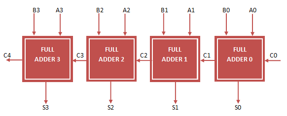
Biz bot 2 games disconnects

In this project, we will design arithmetic circuits using an FPGA. We will build a 4-bit magnitude comparator, a ripple-carry adder, and a multiplier circuit. You can challenge yourself by integrating all of those circuits together with some multiplexers to build an arithmetic logic unit ALU.

A magnitude comparator is a device that receives two N-bit inputs and asserts one of three possible outputs depending on whether one input is greater than, less than, or equal to the other simpler comparators, called equality comparators, provide a single output that is asserted whenever the two inputs are equal.

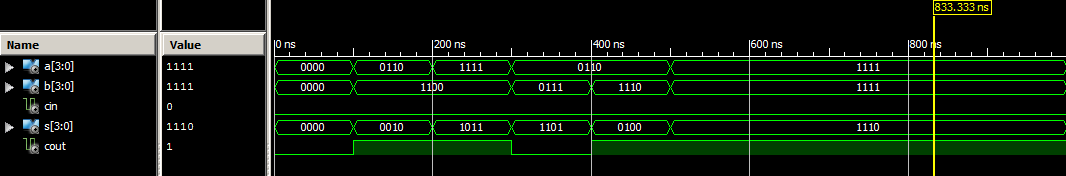
The truth table of a bit-sliced magnitude comparator and the block diagram of a magnitude comparator are shown in Figs. Adder circuits add two N-bit operands to produce an N-bit result and a carry out signal the carry out is a '1' only when the addition result requires more than N-bits. The logic graph in Fig. The highlighted bit pairs and the associated carries show that a bit-slice adder circuit must process three inputs the two addend bits and a carry-in from the previous stage and produce two outputs the sum bit and a carry out bit.

It is possible to capitalize on this observation, and create a smaller bit-slice circuit for use in the LSB position that does not have a carry-in input. The ripple carry adder block diagram is displayed in Fig. Hardware multipliers, based directly on adder architectures, have become indispensable in modern computers.

In this algorithm, one partial product is created for each bit in the multiplier—the first partial product is created by the LSB of the multiplier, the second partial product is created by the second bit in the multiplier, and so forth. The partial product bits need to be fed to an array of full adders and half adders where appropriate , with the adders shifted to the left as indicated by the multiplication example.

The final partial products are added with a CLA circuit. Note that some full-adder circuits bring signal values into the carry-in inputs instead of carry's from the neighboring stage. This is a valid use of the full-adder circuit; the full adder simply adds any three bits applied to its inputs. The circuit for a partial product and the block diagram of the multiplier is shown in Fig. Up to this point, you are expected to be able to describe circuits structurally.

Based on the block diagram shown above in Fig. Before deploying your circuit on your board, write a test bench to verify that your circuit is correct. Unlike the adder and subtractor, multipliers do not have an operator support in Verilog, mostly due to the fact that there are various ways to implement a multiplier which trade off power, hardware resource, and speed.

So implementing a multiplier structurally is the only solution. Back to the list Share: Design Arithmetic Circuits Project Before you begin, you should: Have your FPGA board set up.

Be able to describe digital circuits using logic operators. Be able to write test bench and simulate circuit using ISim. After you're done, you should: Understand how magnitude comparators, ripple-carry adders, and multipliers work.

Be able to describe magnitude comparators, ripple-carry adders, and multipliers structurally. Design a 4-bit Comparator Create a Verilog module for a bit-sliced magnitude comparator according to the truth table presented in Fig. Design a 4-bit Binary Adder Create a Verilog module for a full adder. Design a 4-bit Multiplier Up to this point, you are expected to be able to describe circuits structurally. Now that you've completed this project, try these modifications: Implement a 4-bit borrow ripple subtractor using bit-sliced design methodology and describe it structurally in Verilog.

Inputs and Output of the ALU are 4-bit binary numbers in 2's complement. Other product and company names mentioned herein are trademarks or trade names of their respective companies.